The CoWoP Mandate
- Feb 2
- 10 min read
The AI processor is losing the package substrate to save the timeline. For the rest of the supply chain, it's the new blueprint for value creation.
TL; DR:
Nvidia is pulling CoWoP packaging forward to solve signal integrity problems at 448 Gbps and avoid the assembly reliability issues that plagued Blackwell's cable-based approach.
CoWoP eliminates the package substrate entirely. This excision removes a primary source of electrical signal loss and migrates manufacturing risk upstream, ensuring that failures are identified early in the process rather than at the finish line.
In the AI era, time is value. In AI's compressed profit window, paying premiums for low-yield boards beats risking timeline delays from late-stage assembly failures.
A new value capture model for the supply chain. PCB fabricators, power suppliers, cooling providers, and interconnect manufacturers with the process expertise to master statistically punishing yields will command premiums rather than compete on cost. The ability to manufacture certainty becomes the new currency.
In the exacting technology transitions of semiconductor assembly, timelines are usually glacial, they shift by years, not months. However, a report circulated through the back channels of the sell-side analyst network in January 2026 that abruptly reset the clock. Contrary to the measured engineering consensus that CoWoP (Chip-on-Wafer-on-PCB) was a distant "2027/2028 story," reports suggested that testing had already begun and pilot production was imminent. Nvidia is not waiting. The future has been pulled forward aggressively into late 2026.
CoWoP is an IC packaging method similar to CoWoS. In both methods, the processor chip and memory are mounted on an interposer. But CoWoP has a crucial distinction: the interposer assembly is flip-chip bonded directly onto a platform PCB rather than an ABF (Ajinomoto Build-up Film) substrate. Essentially, CoWoP eliminates the organic ABF substrate and redistributes its functions to the silicon interposer and platform PCB.

To understand the acceleration of CoWoP development, we must look at the Tech Frontier Window. The useful life of AI infrastructure is governed by a depreciation curve that looks like a shark fin: a brief, vertical period of outsized returns followed by a rapid collapse into obsolescence as newer models arrive. In this window, every hour of delay costs millions in hyperscaler revenue that can never be recovered. This changes the entire calculus of component costs.
Some observers view the rationale for CoWoP as a clever maneuver to scale package dimensions and accommodate larger modules. We believe, however, that this perspective reverses cause and effect. While there is no doubt that AI module packages are expanding, the true origin story begins with the migration of interconnects into the platform itself
For the ODMs racing to assemble Nvidia’s Blackwell architecture last year, the moment of clarity came in the form of a copper cable. Nvidia had bet on "twin-ax" cables, dense high-gauge interconnects designed to bypass the signal loss of the PCB and backplane. This wager was motivated by time-to-market constraints, leaning on a supply chain that had been refining the technology for years. They were intended as the bridge to the next era of data rates, holding the line until optical interconnects arrived.
But in the practical reality of server rack assembly, the bridge proved unstable. The cables were bulky, obstructing the precise airflow required to cool critical support components like power shelves, network cards, and management modules. More critically, they introduced an assembly yield crunch. When a cable harness failed during testing, it delayed the Blackwell rollout, teaching the supply chain a sharp lesson: in the Tech Frontier Window, where ROI is made, deployment certainty is paramount.
This vulnerability was destined to escalate in the next generation, where cable assemblies, and potentially optics, would be forced to terminate directly inside the chip package. While the market fixated on the Blackwell delays, a different solution was already taking shape within the engineering labs. A photographed slide leaked under the unassuming acronym CoWoP. The image soon became ubiquitous, sparking commentary from every technologist and analyst in the ecosystem. Early observers were skeptical. They scrutinized the manufacturing complexity, concluding that the approach was inefficient. If it worked at all, they argued, it would merely shift costs, not reduce them.

These critics, however, were looking at the wrong ledger. CoWoP is not a cost-reduction strategy in the traditional sense, nor do we view it merely as a mechanism to facilitate the expansion of processor module dimensions. It is a strategic pivot that prioritizes system-level survival over component-level savings. It signals an opportunity for PCB fabricators to break out of the hypercompetitive commodity era and ascend into the higher-value tier of the Silicon-Adjacent Foundry
The 448Gbps Interconnect Wall
To understand the necessity of CoWoP, one must look at the NVLink interconnect roadmap. Nvidia’s upcoming Rubin architecture will transition from NVLink 5 to NVLink 6, doubling the data rate per lane from 224 Gbps to 448 Gbps.

In the context of signal integrity, 448 Gbps is uncharted territory. At the frequencies required to support this throughput, electrical signals degrade rapidly traversing through copper and dielectric materials. The "Link Budget," the allowance for signal loss between chips, is already tight at 224 Gbps. At 448 Gbps, it becomes almost insurmountable. One of the largest contributors to this signal loss is the ABF package substrate, which connects the silicon to the motherboard. It is the 'oS' component of CoWoS, a layer riddled with vias and impedance mismatches that erode signal integrity before the data even leaves the package. These vias are also a significant loss in the power distribution network to the GPU.
Nvidia has not yet disclosed how it will achieve the step change to 448 Gbps. The prevailing view suggests doubling the Nyquist frequency from 56 GHz to 112 GHz while leaving the modulation at PAM4 and the dual simplex lane intact. However, there is some speculation that they could implement synchronous bi-directional signaling, converting each lane into a full-duplex two-way channel. Both approaches are hard, but in different ways. Doubling the Nyquist burdens the channel; full-duplex burdens the DSP. The engineering choices are stark.
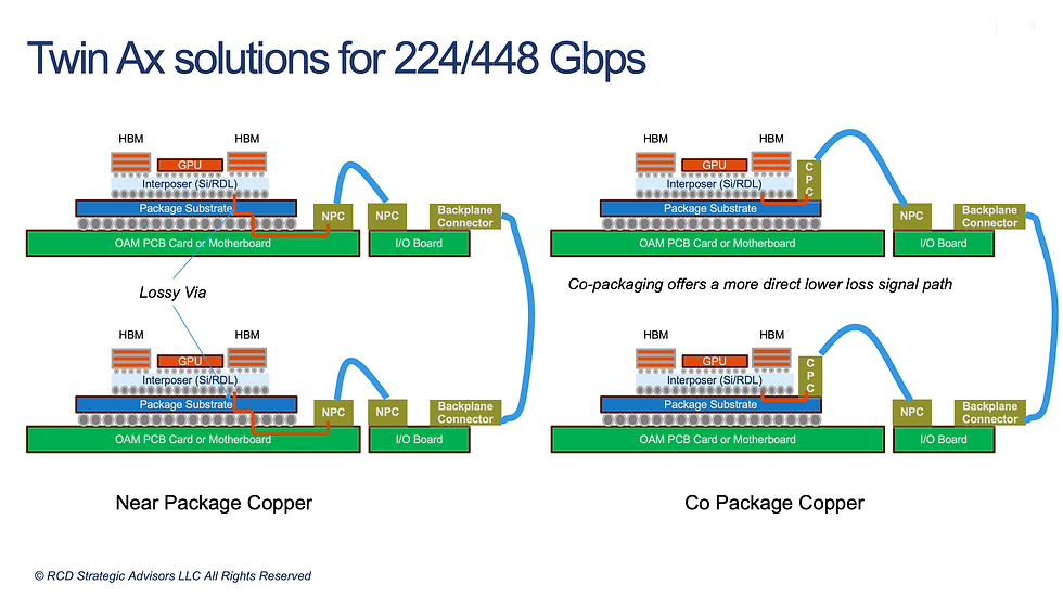
To alleviate channel loss, the component industry proposed "Co-Packaged Copper" (CPC). This appeared to be a logical evolution of the twin-ax cables used to bypass the PCB in current architectures. By terminating twin-ax cables directly onto the package substrate, CPC effectively circumvents the lossy vias of the interposer.

However, this approach swaps a signal integrity problem for another potential downstream yield calamity. Whether the interconnects are hard-soldered or compression-mounted using elastomeric materials, they introduce a critical reliability chokepoint. A soldered connection creates a permanent failure mode where a single bad lane scraps the entire GPU assembly. Alternatively, elastomeric solutions require significant clamping force to maintain contact reliability. This mechanical pressure, combined with the need for physical "beachfront" real estate to house the latching mechanisms magnifies warpage risks and complicates the thermal management.
This physical crowding is an issue for optics as well. While Co-Packaged Optics (CPO) can solve the signal loss problem, the optical transceivers still require structural support at the package boundary. The channel medium may change, but the density challenge remains.
The CoWoP Mandate
The concept of CoWoP is elegant in its subtraction: the complete removal of the ABF package substrate. The Chip-on-Wafer assembly mounts directly onto a high-density 'Platform PCB.' Admittedly, the distinction between a package substrate and a Platform PCB is largely semantic, as both rely on organic laminates. CoWoP has not eliminated the substrate so much as merged the motherboard and package into a massive 'Super-Substrate.'
The brilliance of CoWoP is not merely that it removes a material layer; it is that it fundamentally changes the negotiation between materials. For years, advanced packaging engineers relied on the ABF substrate to act as a shock absorber between the rigid silicon and the thermally chaotic motherboard. It was a necessary compromise, but it was also a fragile one. Silicon is rigid and unforgiving, while the motherboard is organic and expansive. When they heat up, they move at different rates, and the substrate served as the buffer designed to absorb this conflict.
CoWoP abandons this "brute force" buffering in favor of a seamless gradient. Yet this architectural leap is only possible because of the evolution of the interposer itself. The previous standard, CoWoS-S, used a rigid silicon interposer that fought against the natural expansion of the motherboard. That stiffness forced engineers to retain the ABF substrate as a necessary buffer to prevent cracking. The breakthrough arrived with the shift to CoWoS-L. By rebuilding the interposer with organic molding compound, TSMC created an interposer that behaves like the circuit board beneath it. It expands with the platform PCB rather than resisting it. The accelerator module is no longer managing a conflict between hostile materials.
But the most important advantage happens away from the processor. CoWoP allows high-speed interconnects to bypass lossy vias, granting the electrical signal sufficient margin to travel through the Platform PCB to a backplane connector. By erasing the 5-8 dB of signal loss typically consumed by the vias of an organic substrate, CoWoP returns that margin to the system link budget. Effectively, CoWoP is enabling the elimination of twin-ax cables on the motherboard blade and on the backplane. Although Nvidia has not disclosed details, and the design is still in flux, this is the exact architecture that has been suggested for the Rubin Ultra. This approach solves the 448 Gbps signaling problem without incorporating the complexity of twin-ax cables, CPC, or requiring a premature leap to CPO.

Note: For illustration only
However, this elegance comes at a price. The Platform PCB is not standard PCB technology. It requires Modified Semi-Additive Process (mSAP) technology, a method of building copper interconnects up rather than etching them down. This technology is typically reserved for smartphone logic boards and a few 800Gbps optical transceiver boards. Ironically, in a development that served as a technological Trojan horse, twin-ax connector manufacturers began utilizing SLP boards over a year ago to demonstrate Near Package Copper (NPC) solutions.
Applying mSAP over the vast surface area of a GPU module is statistically punishing. The laws of probability and defect density dictate that as the active area increases, yields plummet. Consequently, the cost of the board rises significantly, but in AI's capital economy, that cost is irrelevant compared to the value of time.
The Sharkfin Logic of AI Capital
In the Tech Frontier Window, time-to-market and system reliability are the only metrics that truly matter. Nvidia will pay a premium for lower-yield mSAP boards upstream if doing so prevents ODM assembly yield losses and time-to-market delays downstream.
The logic of CoWoP is the logic of 'Risk Timing': at the cutting edge, yield loss is inevitable, but its timing is controllable. In a Co-Packaged Copper architecture, risk arrives late; it appears only when mounting cables to a finished package, where a single failure stalls delivery. CoWoP moves this risk upstream, trading miles of potential failure points in twin-ax interconnects for acres of expensive Platform PCB area. While these mSAP boards are difficult to yield, fabricators catch defects at electrical test and 'X them out' before attaching silicon. Nvidia is effectively trading a high pile of scrap motherboards (which are cheaper) for a zero pile of stalled Server WIP (which is almost priceless).
Undoubtedly, Nvidia and other AI processor suppliers would have preferred to move the risk even further upstream by connecting larger multichip accelerator modules on the interposer. That leap, however, requires an interposer far larger than what the 300mm CoWoS-L can provide. It would demand a shift to panel-level packaging (TSMC's CoPoS) or glass core substrates, and whether those technologies are ready for Rubin remains an open question.
Rising up to the Silicon-Adjacent Foundry
This shift fundamentally reorders the balance of power within the supply chain. The Platform PCB manufacturer is no longer a commodity "Print Shop" competing on razor-thin margins. They are becoming Silicon-Adjacent Foundries. Like the package substrate makers before them, they are mastering a capital-intensive process critical to the AI server's survival, elevating their status to partners from vendors.
When Apple first drove the development of mSAP-based SLP with its supply chain, it subsidized the capital expenditures for SLP lines to miniaturize the iPhone motherboard. Apple bought down risk from its suppliers by making capital investments on their behalf, demanding a 'Cost-Plus' pricing model where the PCB Fabricator became the process expert under Apple's margin caps.
Nvidia's foray into mSAP for CoWoP is different. The AI hardware value chain offers larger profit pools than smartphones ever did, but the window to capture that profit is measured in quarters, not years. This creates a different calculus: Nvidia will pay premiums to accept upstream yield loss that replaces downstream WIP because under the shark-fin depreciation curve, the cost of delay exceeds any component cost.
But the shift is defined by more than just profit pools and profit windows; it is defined by how the technology reshuffles the burden of yield. It is the practical application of SLP and mSAP technologies that fundamentally reorders the bargaining leverage in the supply chain.
In the micro domain of ABF-based package substrates, the manufacturing process is not static; it's locked in by complexity. Substrate makers anchor the process to guarantee repeatability, forcing the designer to bear the full burden of yield based on strict layout compliance. The designer must adapt to the process. In the macro domain, however, the dynamic inverts. While the design rules for a motherboard are standardized, the physical processing is fraught with variability. Therefore, the fabricator owns the risk, paid to impose order on a chaotic manufacturing process and the process must adapt to deliver the design.
Substrate-like PCBs (SLP) occupy a challenging "hybrid" middle ground, blending the large-scale physical demands of a small motherboard with the micron-scale additive manufacturing techniques of package substrates. This convergence forces a shared responsibility for yield and reliability, resulting in one of the industry's most complex engineering relationships because neither the designer nor the fabricator has total control over the outcome.

This dynamic introduces a new playbook for the broader supply chain. For decades, executives in power electronics, cooling mechanicals, and interconnects operated in a buyer’s market. Their process expertise was commoditized, competitively bargained away by customers who ruthlessly pitted supplier against supplier to shave fractions of a cent. In the smartphone era, a 'chosen few' were selected by platform leaders; the rest fought for scraps.
But when hyperscalers are deploying capital at an industrial scale into a 'Tech Frontier Window' that may close in thirty-six months, the economics of procurement invert. The cost of a component is no longer defined by its bill of materials, but by the risk it removes from the downstream system assembly. In this environment, missile-grade reliability is defined as perfection during the launch/ flight stage rather than longevity beyond the impact. It is not a specification. It is an asset class. The very few fabricators and vendors who can effectively "cheat" the statistical barriers of defect density and thermal physics possess the only leverage that matters: the ability to guarantee time-to-market.

Note: Values approximate and for illustration only; Assumes $8/hr GPU price for stranded revenues
This pattern of value accretion, where suppliers trade yield and reliability for margin, will repeat itself across the ecosystem over the next five years. The technology itself will continue evolving: CoWoP may well mature into CoPoP (Chip on Panel on Platform) as the AI processor-interposer complex scales beyond current reticle limits, requiring even larger platform substrates. Other interconnect approaches may offer better tradeoffs (CPO?, EMIB?, SOW?, Glass-Core?). Material suppliers and thermal engineers who can master the entropy of these massive systems, and assume that burden through their process expertise, will find themselves in the same seat as the mSAP fabricators: no longer vendors, but partners in risk.
The lesson provided by twin-ax integration issues in Blackwell is instructive. In an economy governed by the shark-fin depreciation curve, the only fatal error is a timeline delay. Those who master statistically punishing processes today will be partners tomorrow; those who wait will watch the opportunity pass. The substrate has been erased, but value and function have not disappeared; they have migrated to the hands of those who can manufacture certainty.